Smart Chef Knife

Motivation
Self-tracking and the notion of a "quantified self" is a growing cultural phenomenon, with devices like FitBit, Apple Watch, and smart scales logging when we sleep, how we move, when our heart beats, how much we weigh, and more. The motivations vary, with some measuring for curiosity, and others to quantify attempted improvements to performance or health. With technology capable of logging so much of our daily lives, one space is under-addressed: the kitchen.
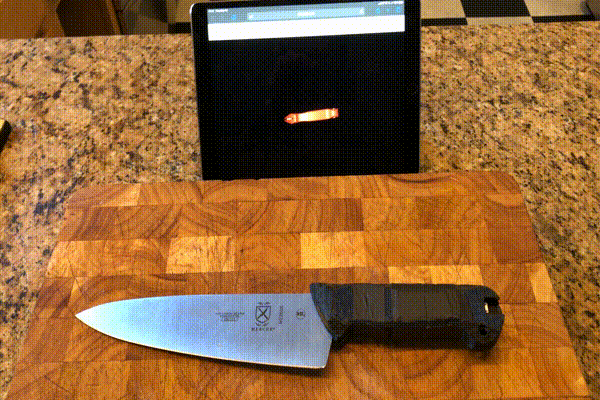
I like to cook, so I wanted to instrument a cutting board and chef knife in order to track how they move. This has the potential for a number of novel uses:
Capabilities envisioned
Variables to track
- Angle while sharpening
- Passes per side while sharpening
- impact (acceleration) while slicing
- orientation while slicing
- time while slicing
Use cases
- tracking wear to the knife and cutting board
- either by time-of-use, aggregate number of slices performed, or some function of load seen
- helps ensure maintenance reflects actual usage
- detect "dullness" by logging when more force is required for slices than we expect
- provide guided step-by-step instruction on how to perform certain operations
- help cooks maintain the right blade angle while sharpening on a whetstone, and track the number of passes per side
- detect orientation, and use accelerometer to log trace of movement, gyro to trace orientation
- users can step through protocolized directions, with the system providing feedback about whether their movements have been performed successfully
- potentially commercializable for restaurant training applications
- tracking performance
- time to complete preparation of one item ("How long does it take me to mince an onion or julienne a carrot? Have I improved?")
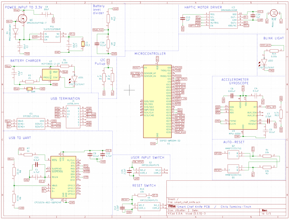
Electronic design
I designed the electronics for the smart chef knife using the free software KiCad.
The KiCad website lists a number of tutorials, which I found helpful for learning the general flow:
- schematic design (describing how components are connected logically)
- "footprint" assignment (describing the physical requirements for component traces and pads)
- PCB layout (physical arrangement of components and connection via copper traces)
- generation of design files for fabrication (2D files describing the copper layers, solder mask layers, silkscreen layers, and hole drill locations)
Schematic design
A necessary step is picking components. Part of that is picking components with the right physical packages. Considerations for my design were:
- I wanted components as small as possible since everything was being crammed into the handle of a chef knife
- Components had to be large enough for me to solder by hand since I don't (currently) have a way to do reflow soldering at home
- Components should have exposed or accessible leads or contacts since I cannot solder under parts or place BGA components
I decided to aim for 0805 (0.08" x 0.05") passive components (capacitors, resistors) where possible because they're small but large enough to easily handle, though I did pick smaller 0603-packages for components there were many of, or components where they needed to be packed near other components.
In a thread on the EEVBlog forum I found a helpful cheatsheet of SMT component sizes:
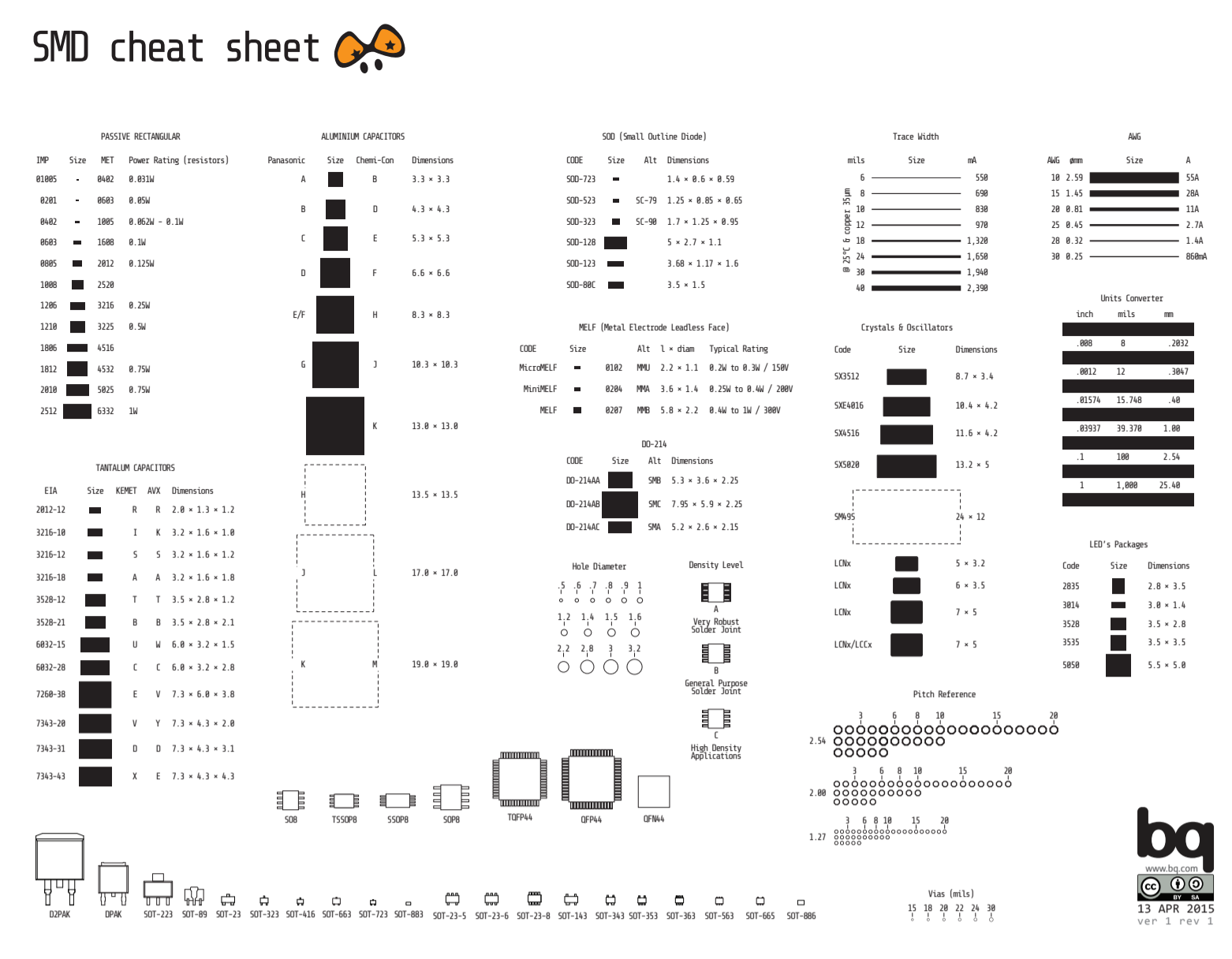 Download: SMD components cheatsheet
To meet my design objectives I knew I needed several components:
- a gyroscope/accelerometer to track motion
- a rechargeable battery (and way to charge it)
- a small motor with an eccentric mass for haptic feedback (and a way to drive it)
- radio modems to communicate over Wi-Fi and/or Bluetooth
- A microcontroller to coordinate all of the components
- a USB connection for programming, charging, and debugging (with USB-to-UART interface)
To meet these needs I chose to use the following components:
- ESP32 Microcontroller, which is powerful and has Wi-Fi and Bluetooth built-in
- MPU-6050 6-axis accelerometer/gyroscope
- MCP73831 battery charger
- DRV2605L haptic motor driver, which can brake motors, apply custom or pre-programmed waveforms, account for physical parameters of motors, and provide appropriate drive current to create sharp haptic feedback
To learn how to integrate the ESP32 into a schematic, I reviewed the example design of the ESP32 development board as well as the Adafruit Huzzah32 ESP32 board. There's not much to them, so my design was mostly about adding the gyroscope/accelerometer chip and connecting all of the other components.
There was one curious part of both example ESP32 designs it took me a while to understand (excerpt from the dev board schematic):
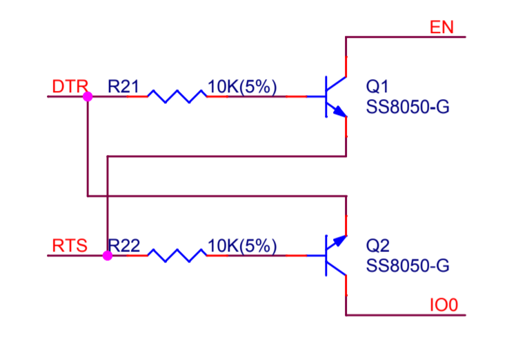
This is the reset circuit. The key information to understand is can be found on a GitHub page describing boot mode selection, which says "The ESP32 will enter the serial bootloader when GPIO0 is held low on reset." Ah ha. The DTR line from the UART connection sinks current, allowing the GPIO0 to be brought low on the ESP32, triggering a reset via active EN when RTS is high.
The truth table for the reset progression looks like this:
| DTR | RTS | ---> | EN | IO0 |
|---|---|---|---|---|
| 1 | 1 | 1 | 1 | |
| 0 | 0 | 1 | 1 | |
| 1 | 0 | 0 | 1 | |
| 0 | 1 | 1 | 0 |
The same page goes into a bit more detail:
"Some third party ESP32 development boards use an automatic reset circuit for EN & GPIO pins, but don't add a capacitor on the EN pin. This results in unreliable automatic reset, especially on Windows. Adding a 100nF (or higher) value capacitor between EN pin and GND may make automatic reset more reliable."
So maybe that's why the cheap ESP32 dev board I ordered from AliExpress does not reset reliably. I made sure to include a larger capacitor between EN and GND (2.2pF).
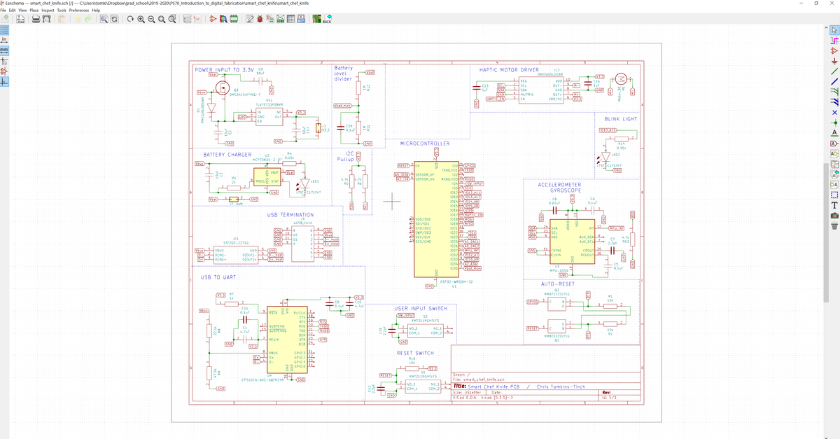
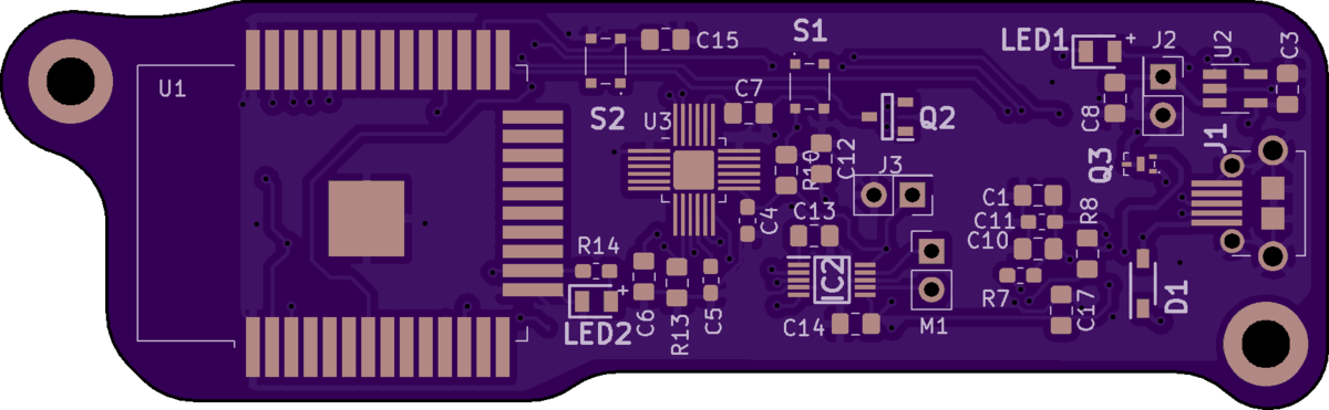
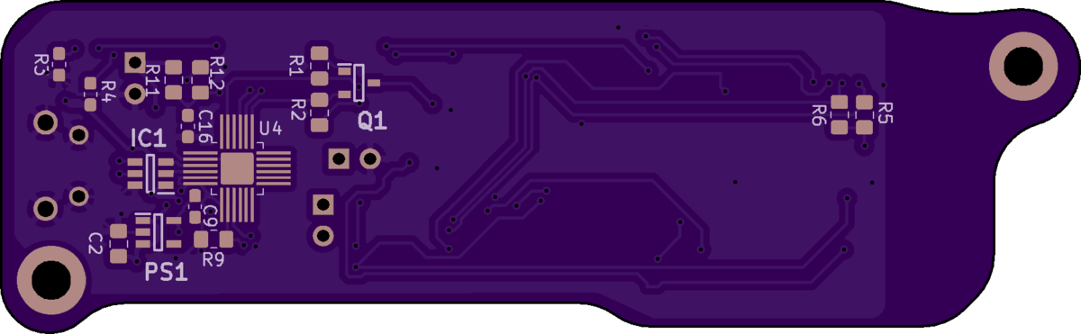
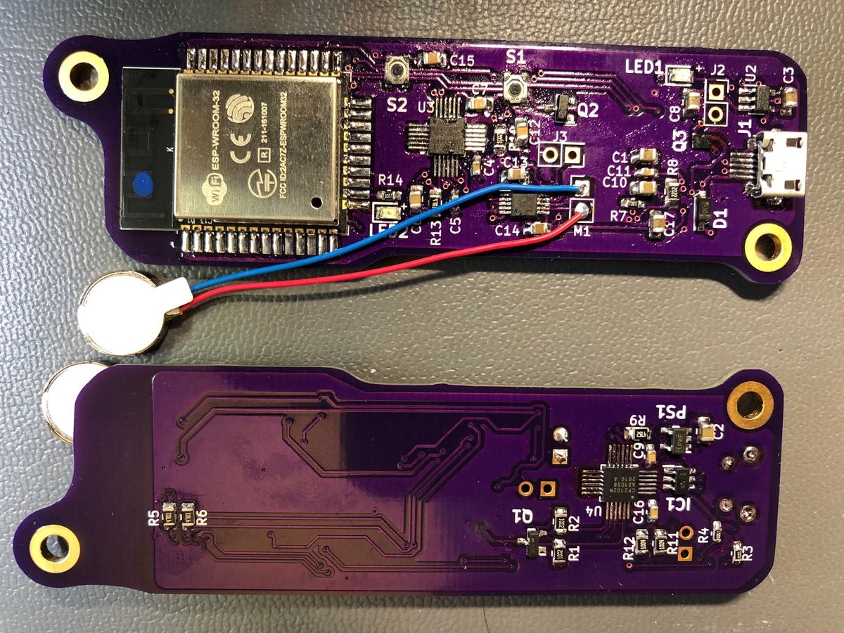
When I was done my schematic looked like this:
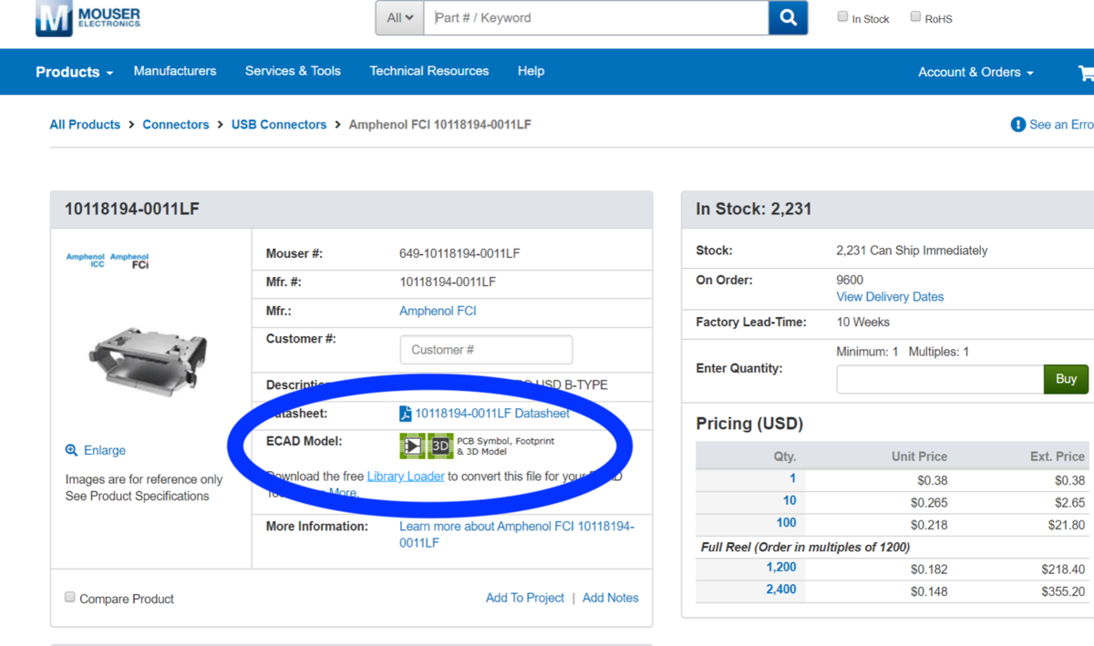
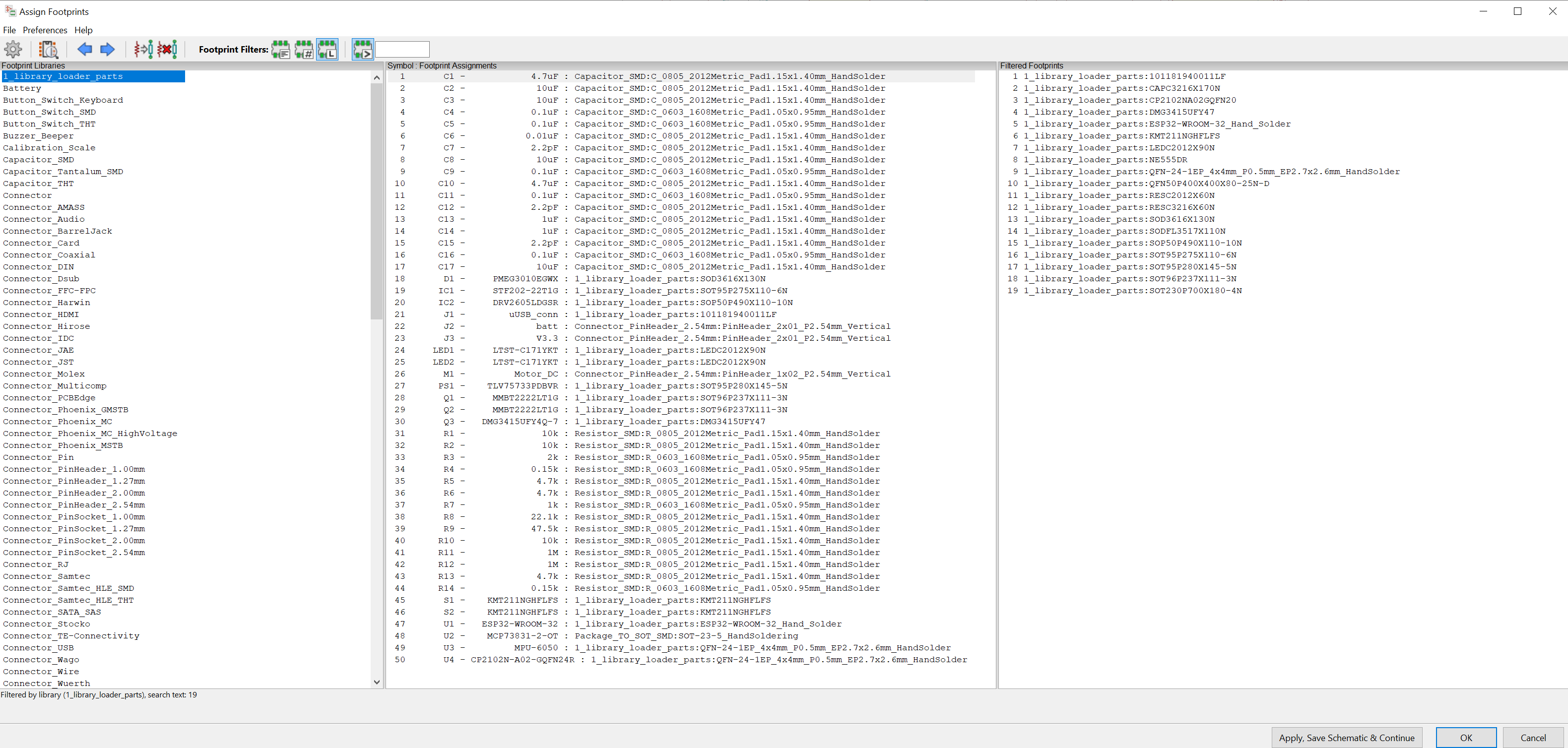
For assigning component footprints, component vendors like Mouser and DigiKey now helpfully provide footprint and 3D models for many components. This makes it a breeze to include most commercially-available components in a design: the KiCad schematic editor can easily know how many pins a component has, what they're labeled, and which pin numbers those labels correspond to. It also makes layout easier because the same component files describe the physical footprints needed by the components.
⬆ this is amazing.
I did have to assign foot prints for many components myself, but fortunately most of these were standard and built-in to KiCad. I was thankful Mouser had the footprint for my microUSB connector.
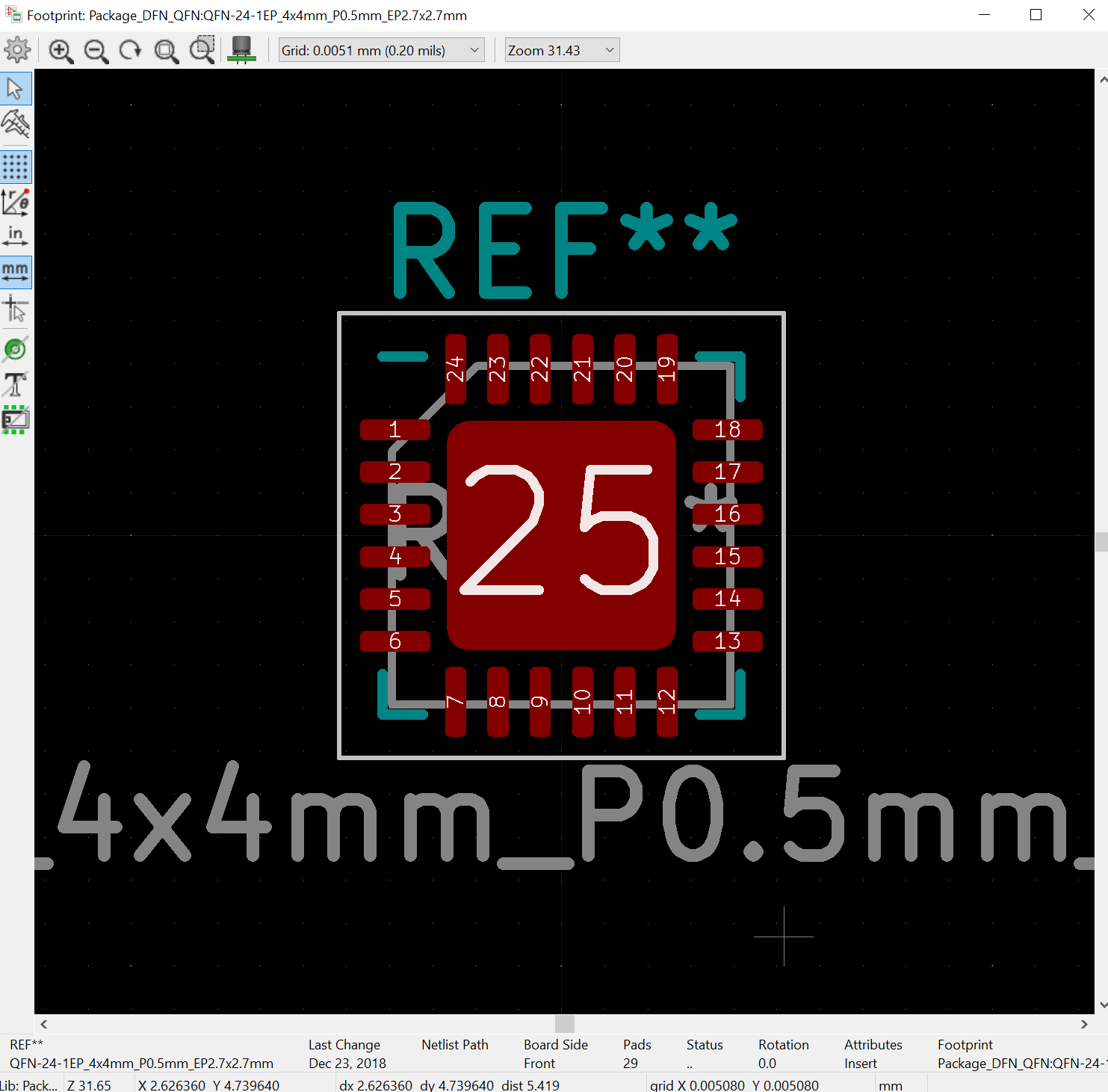
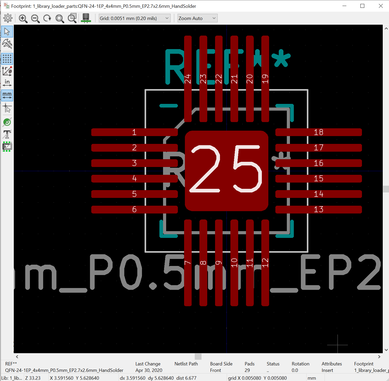
In addition to assigning footprints, I modified a few to make them easier to hand solder by extending the length of the copper pads to the point where I could access them with a soldering iron. Here is an example of my modified QFN24, before and after adjustment for hand soldering:
PCB layout & fabrication files
After freezing the schematic it's time to lay out the components physically in a way that I can fit the board within the handle of a knife.
The first step of laying out a PCB is to define the external geometry of the board. The external bounds constrain where components can be placed and it's best to set them at the start. I started by drawing the approximate shape of a knife handle on paper:
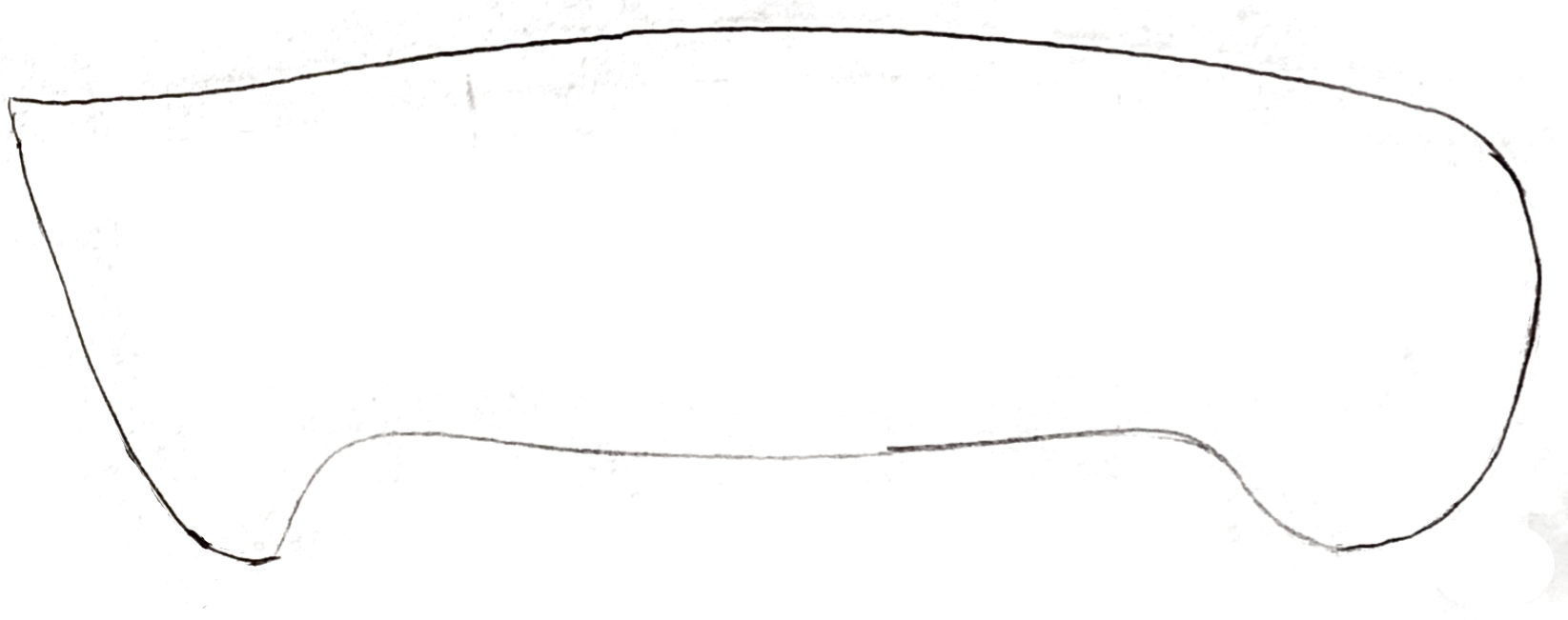
I took a photo of my drawing, imported it into Inkscape, and traced over my rough lines with crisp digital ones. I then exported the resulting line drawing in dxf format so I could import the outline into KiCad. Of note is that in order to get the scaling right I had to export the drawing in inches, and temporarily set my KiCad layout to inches for the import.
I imported the design rules for the fabricator, OSH Park, from this repository from one of the lead developers of KiCAD.
In KiCad I prefer the "legacy" toolset; the "modern" toolset cannot show logical "ratsnest" connections for only the selected part, whereas the legacy toolset can do so. This is a regression set to be corrected on the development roadmap.
The import worked, and my hand sketch of the board outline now existed in the same digital world where I could place electronic components:
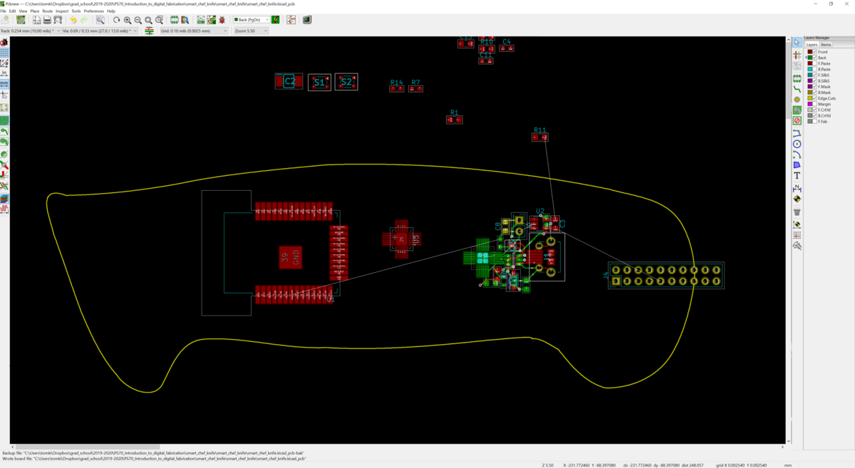
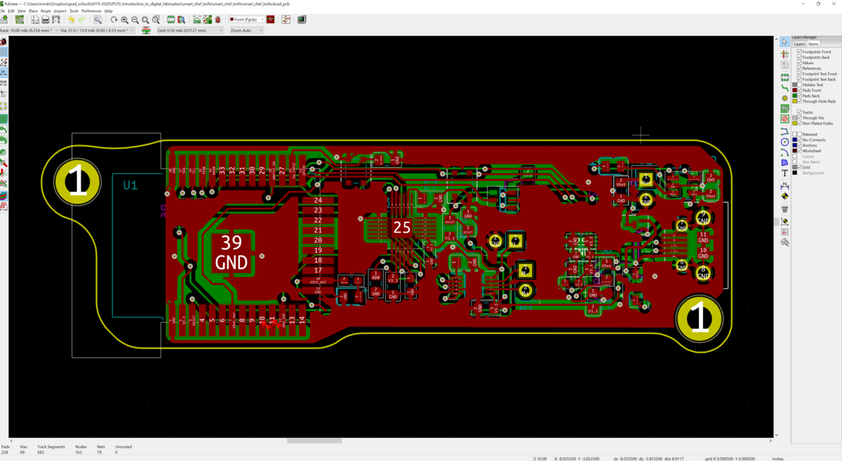
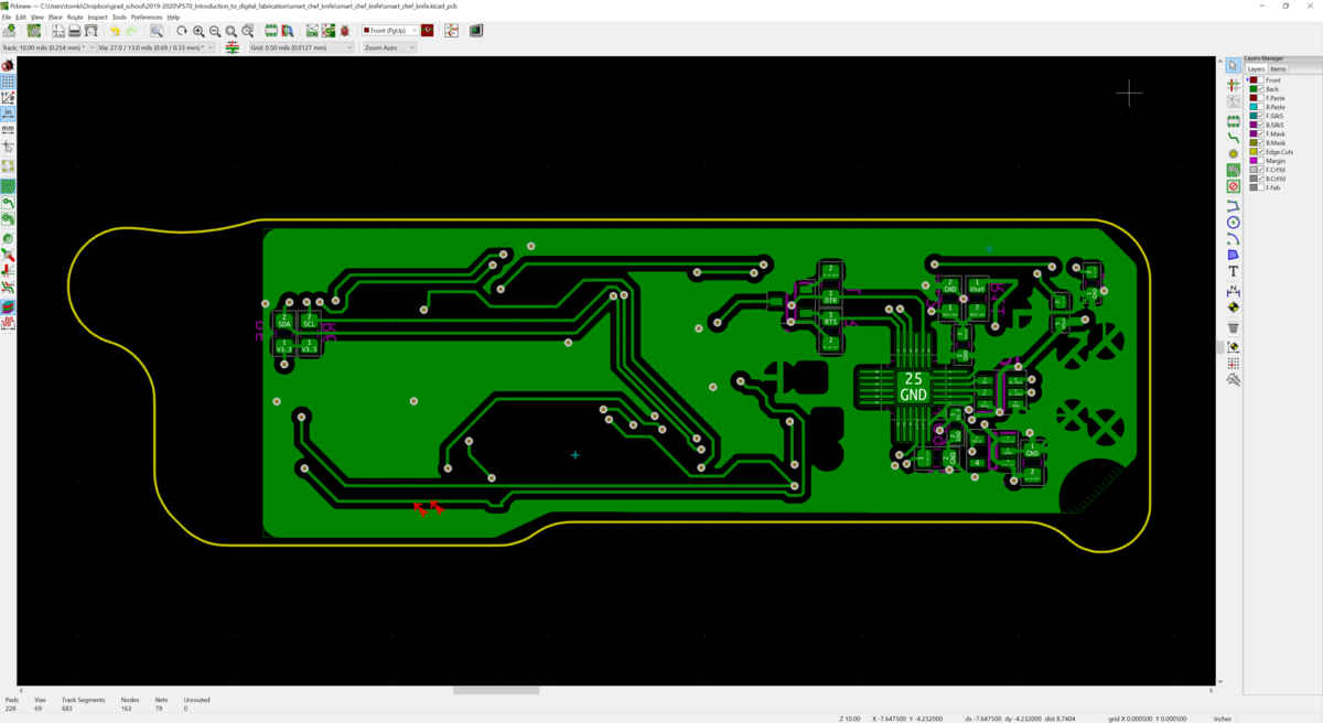
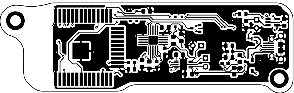
From here it was a matter of dragging and dropping components around until they fit together. KiCad helpfully provides a "ratsnest" view that carries over logical connections between component pins ("nets" in EDA parlance) from the schematic editor. The ratsnest view makes it easier to see which components are connected, and how they should be rotated (or moved to the back of the PCB) to minimize crossing lines. Here is a small sub-section showing the microUSB connector and the USB-to-UART interface to which it connects. For this particular sub-circuit, it made sense to put the USB connector on the front of the board (where it is accessible), and the USB-to-UART chip on the back of the board (so traces did not need to cross over each other). Red represents copper on the front of the board, green the back.
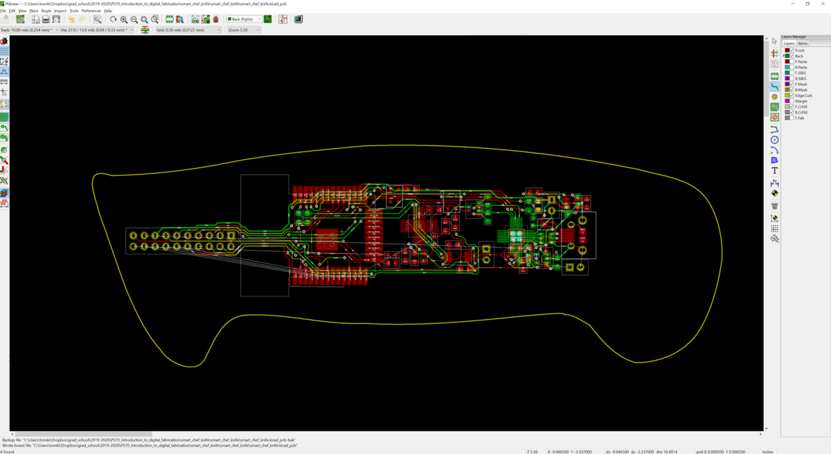
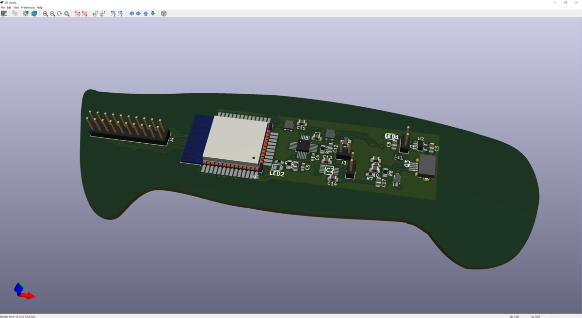
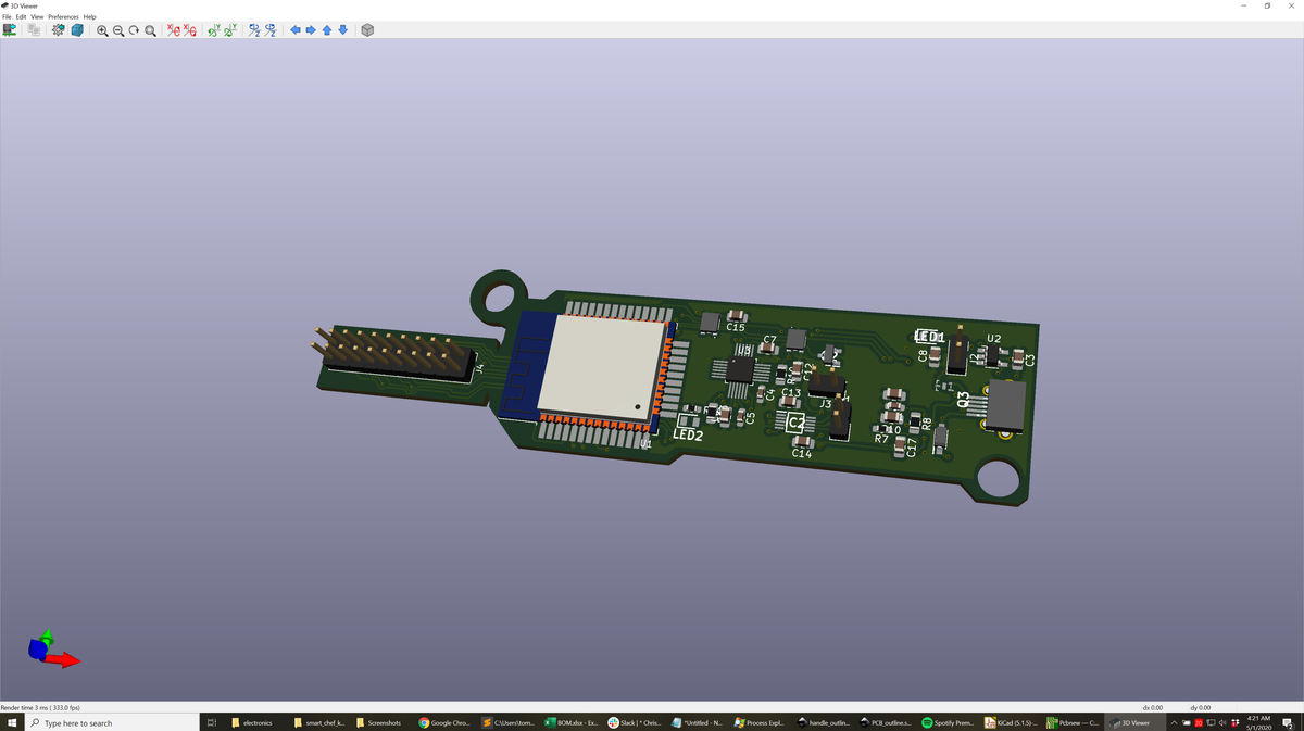
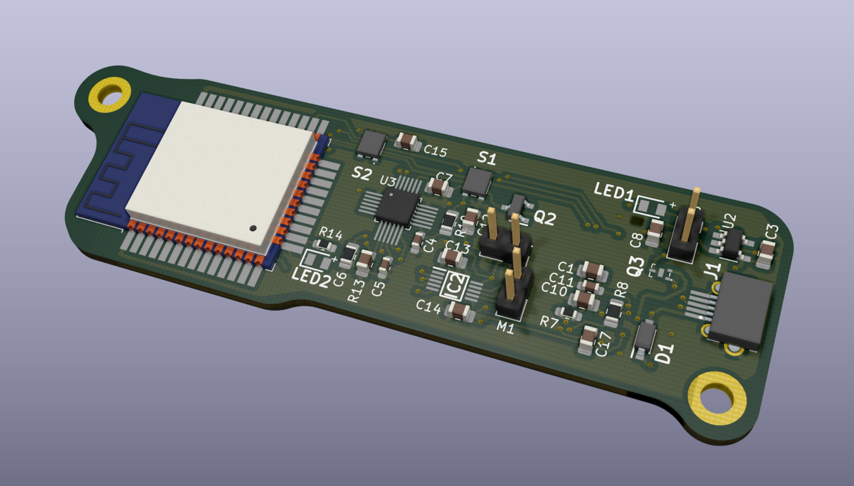
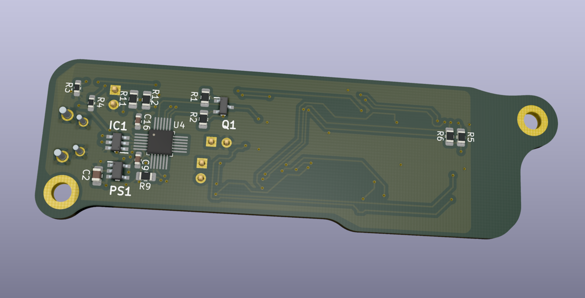
Since KiCad is aware of the package dimensions of all of the components—either because they're standard built-in sizes, or because the component models have been downloaded from a vendor like Mouser or DigiKey—KiCad can generate and render a 3D-model of the PCB. This will become important later on. At this point I could visualize my board. It looked OK, but it could be better:
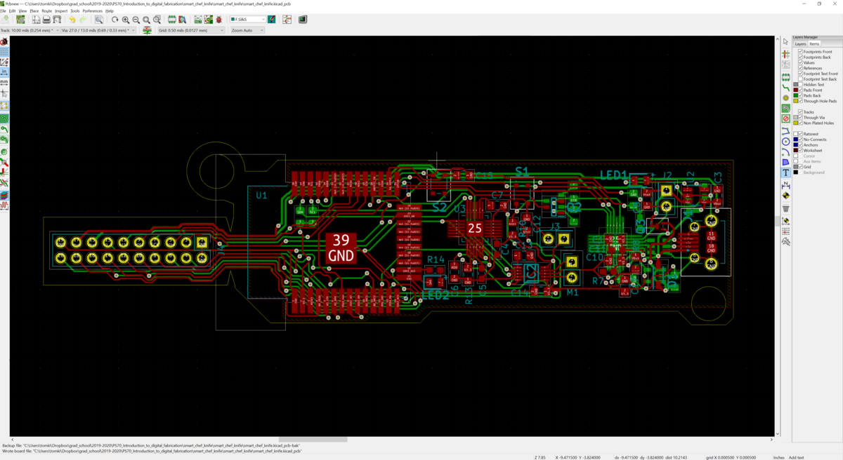
The first problem is that the board is too large. I did a reasonably good job condensing the components to a small area, but the outline of the board itself needs to fit inside a knife handle, not be a knife handle. I trimmed the edge lines to follow the convex hull of my circuit layout, with a few extra warts to accomodate mounting holes:
This looked better, and had a fun electric guitar look to it.
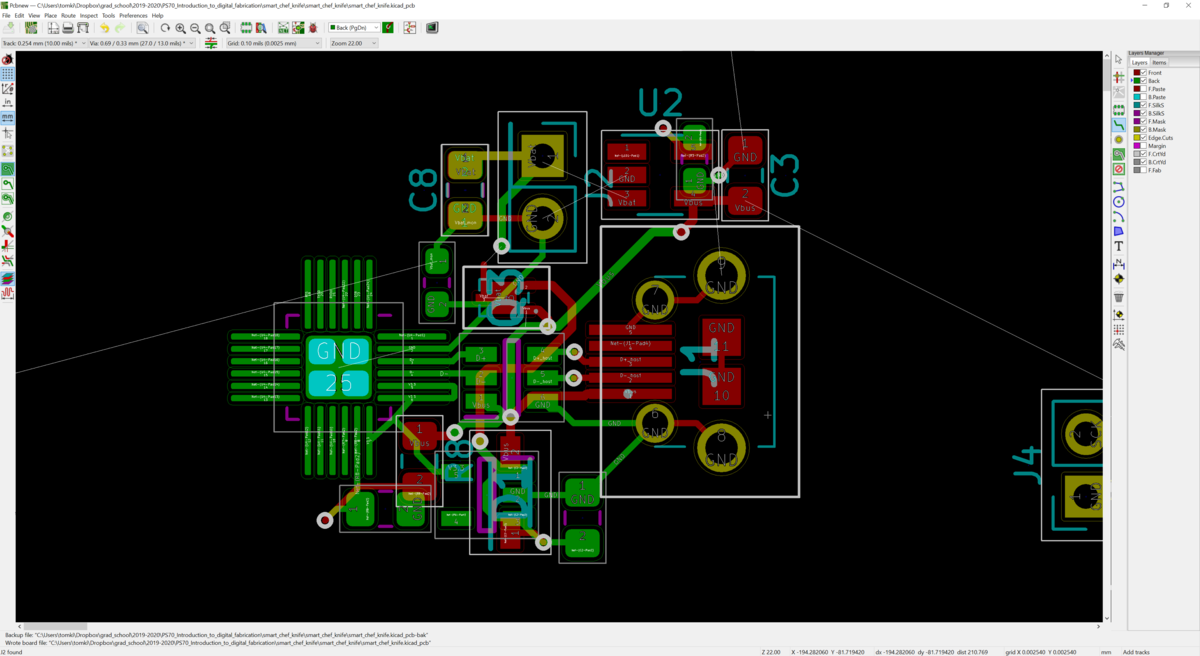
There was another glaring issue, though. I had wanted to break out all of the pins on the ESP32 so I could use this same board for other projects if necessary, hence the large pin header jutting off to the side. It is at this point that I re-read the ESP32 datasheet and learned copper traces and layers need to stay away from a "keepout area" around the build-in antenna. Sadly, the breakout header with all of the pins had 20 traces running through the keepout area, with no way to re-route within knife handle geometry. It needed to go. I removed it, and trimmed down the outline even more. It is at this point that I exported the "edge cuts" layer in KiCad as a dxf file, imported it into Rhino, smoothed out the curves, and re-imported the outline as dxf into KiCad. This cleaned it up. I also learned that mounting holes have their own component class, MountingHole, that results in plated holes rather than drilled ones.
I selected MountingHole:MountingHole_3.2mm_M3_DIN965_Pad to accommodate M3 screws, and replaced my "edge cut" holes with MountingHole objects. These can be placed directly from the PCB layout editor, and do not need to be assigned as footprints to schematic objects unless they need to be electrically connected. From here I added "filled zones" around my schematic design on both sides, connected to ground. Doing so allows for easy connection to ground for many of the components, provides some safety against shorting through components, and helps create a ground plane to reduce electrical noise.
(animation created based on this helpful post, with source adapted from here)
The board looked great!
From here, Gerber files can be exported describing the various layers the final board will have: copper layers for the conductors, solder mask layers to ensure solder only wets the copper below components, silkscreen layers for labels and text, and a list of the positions and sizes of drilled holes. These are Gerber-format files that translate into the 2D designs used to create photo-lithography masks during fabrication for chemical etching as well as application of solder mask and silkscreen ink.
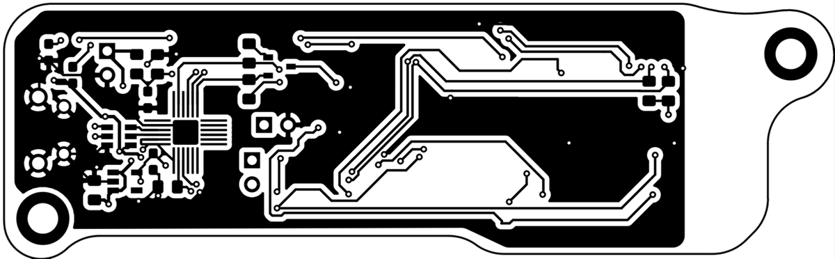
With gerber files in hand, creating a physical board is a matter of either fabricating the circuit boards on one's own, or paying someone else to create them. For the sake of expediency, because I had fine-pitch parts with 0.5mm traces, and because of SARS-CoV-2 related restrictions, I sent my design files to OSH Park for fabrication.
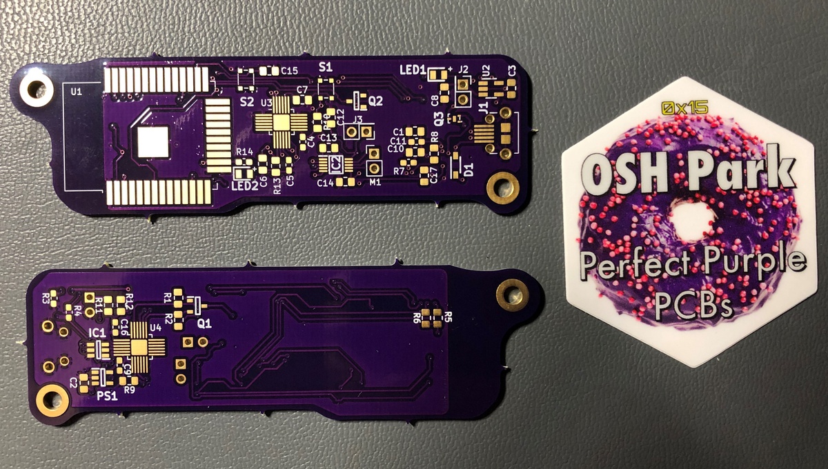
OSH Park is a small group in Portland, OR, that pools small-run PCB orders together onto panels and sends them to a US-based manufacturer for fabrication. The cost is reasonable: $5/in^2 for 3 copies (or $10/in^2 if you're in a hurry). OSH Park boards are seen all over the DIY and open hardware world, and are recognizable for the distinct purple color of their solder mask. In contrast to PCBs created by some other suppliers, boards from OSH Park have gold-plated contacts that are extremely flat and immune to oxidation. That makes it easy to place and solder tiny components in just the right places.

KiCAD generates gerber and drill files, then you just drag and drop a zip file of all of them to OSH Park and they show a render of the finished board:
Then it's a matter of waiting for the boards to be made and mailed. They arrived looking great!
Bill of Materials (BOM) for electronics
| description | chemistry / type | package | vendor | mfg part number | mfg | mouser part # | value | tolerance | qty | reference | unit ($) | ext ($) | 1k pricing ($) | ext 1k | datasheet | note |
|---|---|---|---|---|---|---|---|---|---|---|---|---|---|---|---|---|
| 4.7uF | X5R MLCC | 0805 | Mouser | VJ0805G475KXYTW1BC | vishay | 77-VJ0805G475KXYTBC | 4.7uF | 10% | 2 | "C1, C10" | 0.22 | 0.44 | 0.136 | 0.272 | ||
| 10uF capacitor | X5R MLCC | 0805 | Mouser | VJ0805G106KXYTW1BC | vishay | 77-VJ805G106KXYTW1BC | 10uF | 10.00% | 4 | "C2, C3, C8, C17" | 0.12 | 0.48 | 0.074 | 0.296 | for RC circuit on EN pin of ESP32 | |
| 0.1uF cap | X7R MLCC | 0603 | Mouser | VJ0603Y104JXJCW1BC | vishay | 77-VJ0603Y104JXJCBC | 0.1uF | 5.00% | 5 | "C4, C5,C9, C11, C16" | 0.13 | 0.65 | 0.026 | 0.13 | for decoupling and also for RC circuit on EN pin of ESP32 | |
| 0.01uF capacitor | X7R MLCC | 0805 | Mouser | VJ0805Y103MXACW1BC | vishay | 77-VJ0805Y103MXACBC | 0.01uF | 20% | 1 | C6 | 0.17 | 0.17 | 0.03 | 0.03 | ||
| 2.2pF capacitor | X7R MLCC | 0805 | Mouser | VJ0805A2R2BXAPW1BC | vishay | 77-VJ0805A2R2BXAPBC | 2.2pF | 5% | 3 | "C7, C12, C15" | 0.19 | 0.57 | 0.041 | 0.123 | ||
| schottky protection diode | n/a | SOD-123 | Mouser | PMEG3010EGWX | nexperia | 841-PMEG3010EGWX | 1 | D1 | 0.31 | 0.31 | 0.061 | 0.061 | https://www.mouser.com/datasheet/2/916/PMEG6010CEGW-1599909.pdf | |||
| ESD/TVS diodes for USB lines | 5.25V bidirectional | TSOP-6 | Mouser | STF202-22T1G | On Semi | 863-STF202-22T1G | 1 | IC1 | 0.57 | 0.57 | 0.22 | 0.22 | https://www.mouser.com/datasheet/2/308/NUF2101M-D-1814465.pdf | |||
| haptic control module DRV2605L | MSOP-10 | Mouser | DRV2605LDGSR | TI | 595-DRV2605LDGSR | 1 | IC2 | 2.66 | 2.66 | 1.34 | 1.34 | |||||
| micro usb connector | Mouser | 10118194-0011LF | amphenol | 649-10118194-0011LF | 1 | J1 | 0.38 | 0.38 | 0.182 | 0.182 | ||||||
| "JST connector, 2mm pitch PH series" | ???? | ???? | 1 | J3 | 0 | 0 | ||||||||||
| yellow LED | 0805 | Mouser | LTST-C171YKT | 859-LTST-C171YKT | 2 | "LED1,LED2" | 0.3 | 0.6 | 0.054 | 0.108 | ||||||
| haptic feedback motor | 10mm dia x 2mm disc | Amazon | n/a | n/a | 1 | M1 | 0 | 0 | https://smile.amazon.com/tatoko-10mmx2mm-Vibration-Button-Type-Vibrating/dp/B07NPXD53V/ref=psdc_306577011_t1_B07TX9VG1R#customerReviews | |||||||
| 3.3V LDO | n/a | SOT-223-3 | Mouser | TLV75733PDBVR | on semi | 595-TLV75733PDBVR | 1 | PS1 | 0.58 | 0.58 | 0.202 | 0.202 | http://www.ti.com/general/docs/suppproductinfo.tsp?distId=26&gotoUrl=http%3A%2F%2Fwww.ti.com%2Flit%2Fds%2Fsymlink%2Ftlv757p.pdf | |||
| BJT | SOT-23-3 | Mouser | MMBT2222LT1G | 863-MMBT2222LT1G | 2 | "Q1,Q2" | 0.12 | 0.24 | 0.027 | 0.054 | https://www.mouser.com/datasheet/2/308/MMBT2222LT1-D-1811600.pdf | |||||
| Vbat disconnect MOSFET | Mouser | DMG3415UFY4Q-7 | 621-DMG3415UFY4Q-7 | 1 | Q3 | 0.5 | 0.5 | 0.15 | 0.15 | |||||||
| 10k resistor | thick film | 0805 | Mouser | CRCW080510K0FKEAC | vishay | 71-CRCW080510K0FKEAC | 10k | 1% | 3 | "R1, R2, R10" | 0.1 | 0.3 | 0.01 | 0.03 | ||
| 1M resistor | 0805 | Mouser | CRCW08051M00FKEAC | vishay | 71-CRCW08051M00FKEAC | 1M | 1% | 2 | "R11,R12" | 0.1 | 0.2 | 0.01 | 0.02 | https://www.mouser.com/datasheet/2/427/crcwce3-1762584.pdf | ||
| 2k resistor | thick film | 0603 | Mouser | CRCW06032K00FKEAC | vishay | 71-CRCW06032K00FKEAC | 2k | 1 | 1 | R3 | 0.1 | 0.1 | 0.004 | 0.004 | ||
| 150 ohm resistor | 0603 | Mouser | CRCW0603150RFKEAC | vishay | 71-CRCW0603150RFKEAC | 0.15k | 1% | 2 | "R4,R14" | 0.1 | 0.2 | 0.004 | 0.008 | |||
| 4.7k resistor | thick film | 0805 | Mouser | CRCW08054K70FKEAC | vishay | 71-CRCW08054K70FKEAC | 4.7k | 1% | 3 | "R5, R6, R13" | 0.1 | 0.3 | 0.01 | 0.03 | ||
| 22.1k resistor | thick film | 0805 | Mouser | CRCW080522K1FKEAC | vishay | 71-CRCW080522K1FKEAC | 22.1k | 1% | 1 | R8 | 0.16 | 0.16 | 0.01 | 0.01 | ||
| 47.5k resistor | thick film | 0805 | Mouser | CRCW080547K5FKEAC | vishay | 71-CRCW080547K5FKEAC | 47.5k | 1% | 1 | R9 | 0.16 | 0.16 | 0.01 | 0.01 | ||
| Pushbutton switch | prop. | Mouser | KMT211NGHFLFS | C&K | 611-KMT211NGHFLFS | 2 | "S1, S2" | 0.55 | 1.1 | 0.35 | 0.7 | https://www.mouser.com/datasheet/2/60/kmt2-1382788.pdf | ||||
| ESP32-WROOM-32 | prop. | Mouser | ESP32-WROOM-32 | Espressif | 356-ESP-WROOM-32 | 1 | U1 | 3.8 | 3.8 | 3.8 | 3.8 | https://www.mouser.com/datasheet/2/891/esp32-wroom-32_datasheet_en-1510934.pdf | ||||
| battery charger | Mouser | 579-MCP73831T-2ACIOT | MCP73831T-2ACI/OT | 1 | U2 | 0.56 | 0.56 | 0.42 | 0.42 | https://www.mouser.com/datasheet/2/268/20001984g-846362.pdf | ||||||
| accelerometer/gyro | QFN24 | Mouser | MPU-6050 | 410-MPU-6050 | 1 | U3 | 7.28 | 7.28 | 4.08 | 4.08 | https://invensense.tdk.com/wp-content/uploads/2015/02/MPU-6000-Datasheet1.pdf | |||||
| USB to TTL serial | QFN24 | Mouser | CP2102N-A02-GQFN24R | Silicon Labs | 634-CP2102NA02QFN24R | 1 | U4 | 1.35 | 1.35 | 1.17 | 1.17 | https://www.mouser.com/datasheet/2/368/cp2102n-datasheet-1634912.pdf | ||||
| 1uF cap | X7R MLCC | 0805 | Mouser | VJ0805Y105JXQTW1BC | vishay | 77-VJ0805Y105JXQTBC | 1uF | 2 | "C13,C14" | 0.15 | 0.3 | 0.072 | 0.144 | |||
| 1k resistor | thick film | 0603 | Mouser | CRCW06031K00FKEAC | vishay | 71-CRCW06031K00FKEAC | 1k | 1% | 1 | R7 | 0.01 | 0.01 | 0.004 | 0.004 |
Download: Smart-chef-knife_BOM.xlsx
Physical assembly
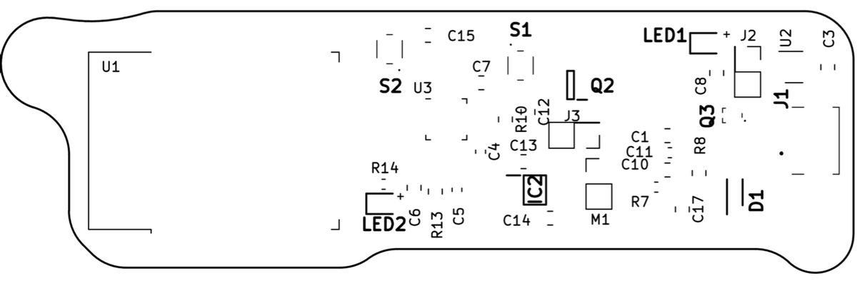
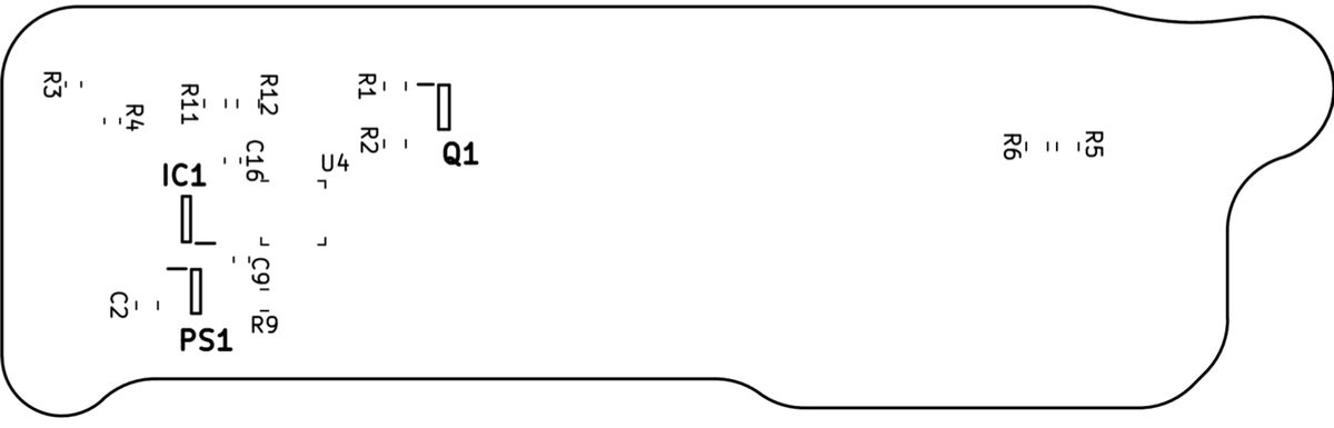
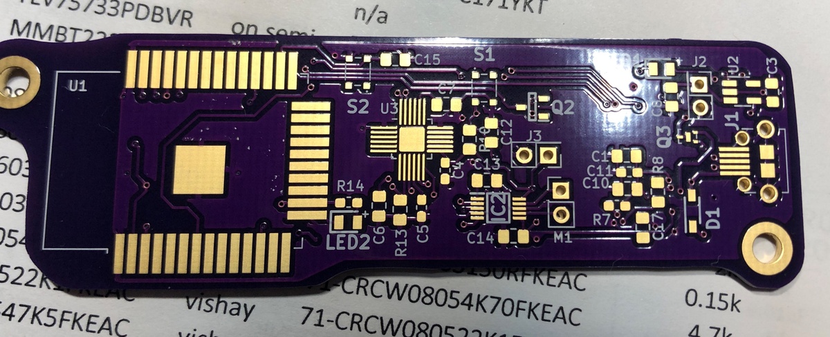
As I mentioned, I was hand-soldering these. I found it helpful to print out the silkscreen layers from KiCad so I could see where on the boards the components should go and so I could cross them off with a pencil as I went. I also printed a copy of the BOM so I could match component part numbers to PCB references.
It's here that I embarked on a bit of a yak shaving adventure. Some of the parts I planned to include are tiny. Really tiny. The pads on a QFN24 part are just 0.5mm wide, separated by 0.5mm. I decided I needed a way to see the small components better while I solder, and more importantly, to inspect my soldering job to check for incomplete or bridged connections. I found a Bausch & Lomb StereoZoom 4 binocular microscope (made in Rochester, NY) on eBay for a great price, and bought it. It needed some cleaning of the optical path but worked perfectly. With the native zoom range of 0.7X - 3.0X and 10x eyepieces, the microscope affords magnification of 7x - 30x.
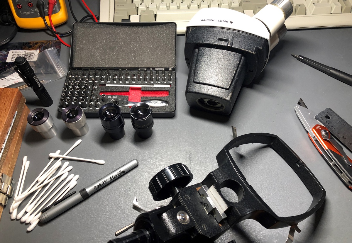
The microscope came with a focusing rack, but unfortunately no stand. The boom arm connector it did have happened to perfectly fit the PanaVise 350 stand I had from leatherworking projects. (I did eventually find a similarly affordable stand on eBay). I was set to solder!
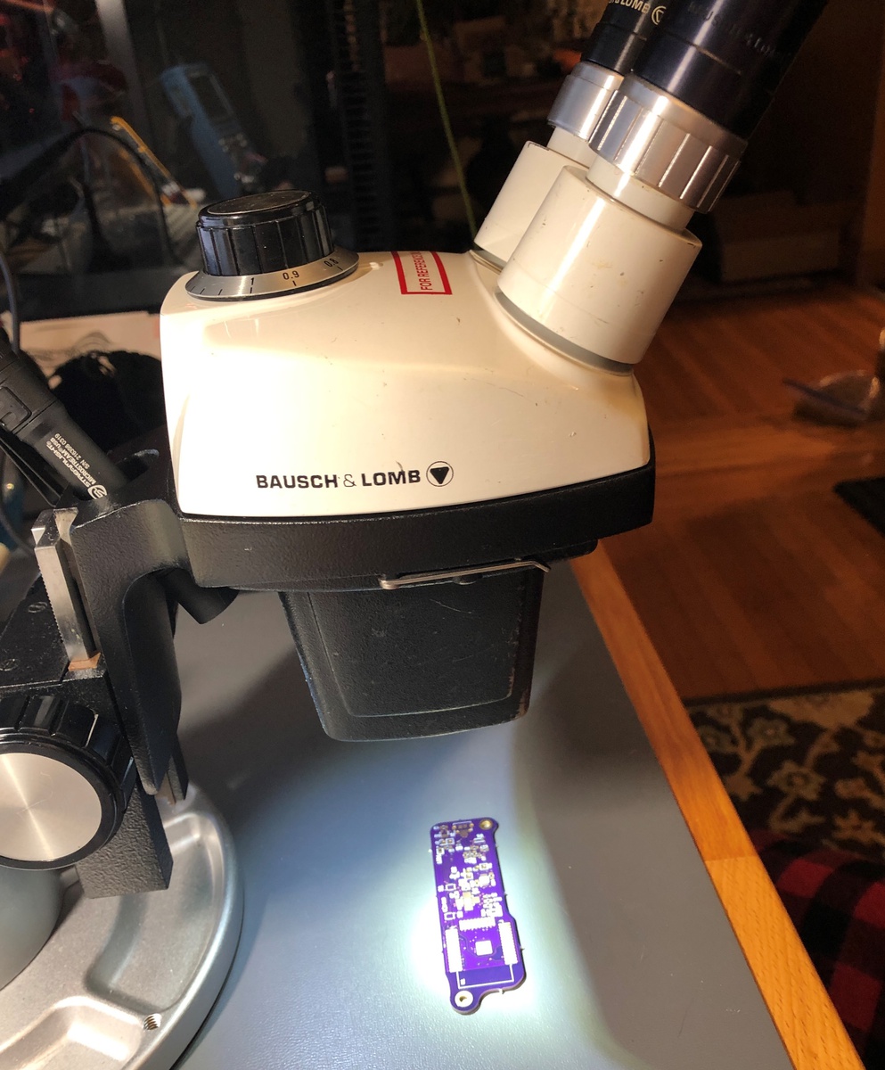
With the microscope I could easily see the 0.5mm QFN pads:
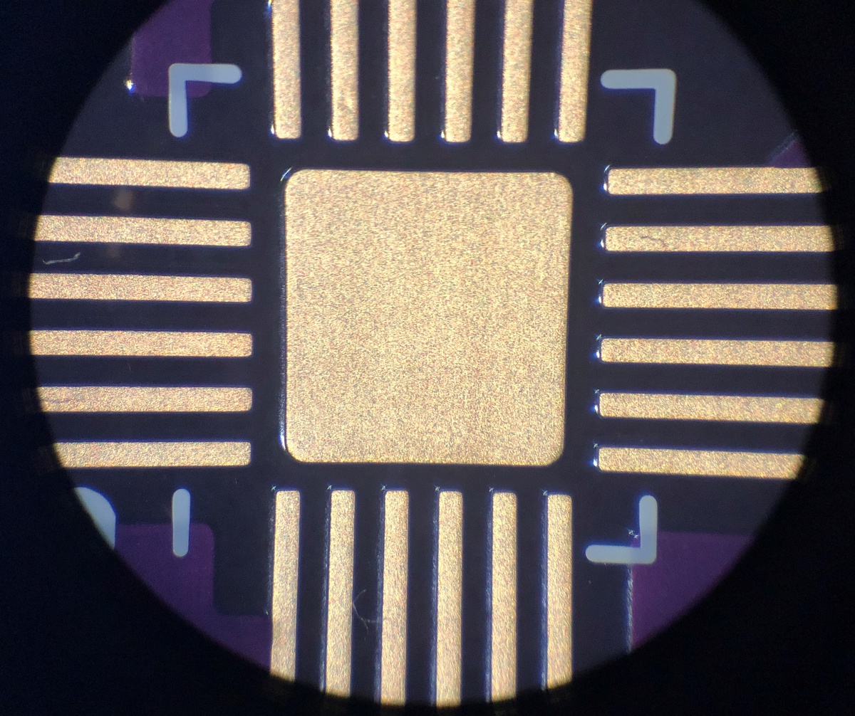
For the QFN parts I found it easiest to place the component as carefully as I could, solder one pin, then check the alignment of all of the pins. If all looked well, I finished soldering the part. If not, I de-soldered the starting pin, re-adjusted the placement, and tried again. Desoldering braid was helpful in this process, as was a flux pen. Eventually the QFN parts were soldered:
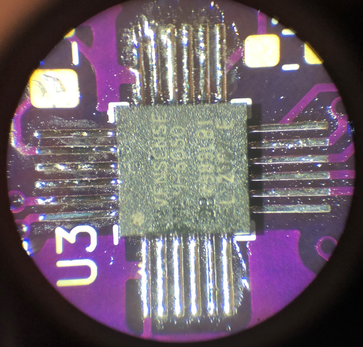
I started with the most difficult parts to solder: the QFN parts, the tiny transistors, and the small surface-mount components before moving on the larger components. Soldering in this order ensured I had room to be extra careful with the most difficult components. Eventually it all came together:
Knife integration design
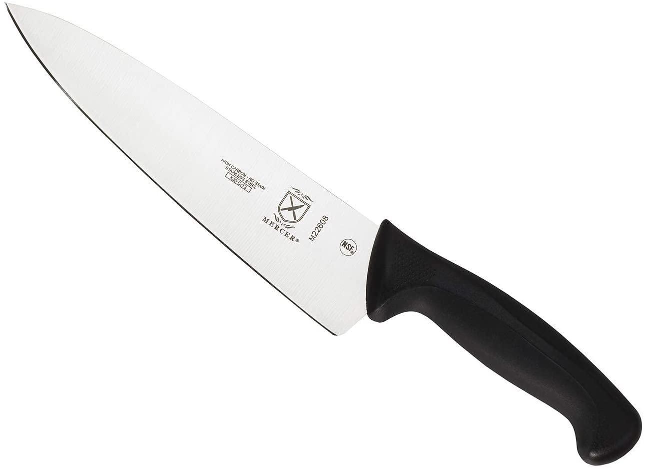
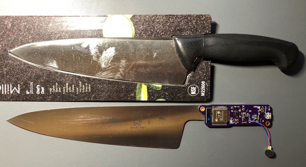
From here I needed to integrate the circuit board I had made with a chef knife. I chose to prototype using a very inexpensive knife from Amazon. Knowing I would need to remove the original handle from whichever knife I chose, I started my knife selection process by trying to find one that had negative reviews stating the handle slipped off easily (so I would have less work to do). That search came up empty, so I went with one that reviewed well and was inexpensive, the Mercer Culinary M22608.
It arrived and a pair of landscaping bypass cutters made quick work of removing the original handle:
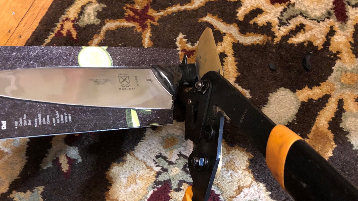
Removing the handle exposed the tang of the knife:
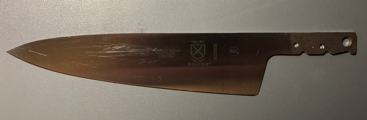
Placing my board on the tang made it clear it would fit in a handle about the same size as the original handle. This was shaping up to work!
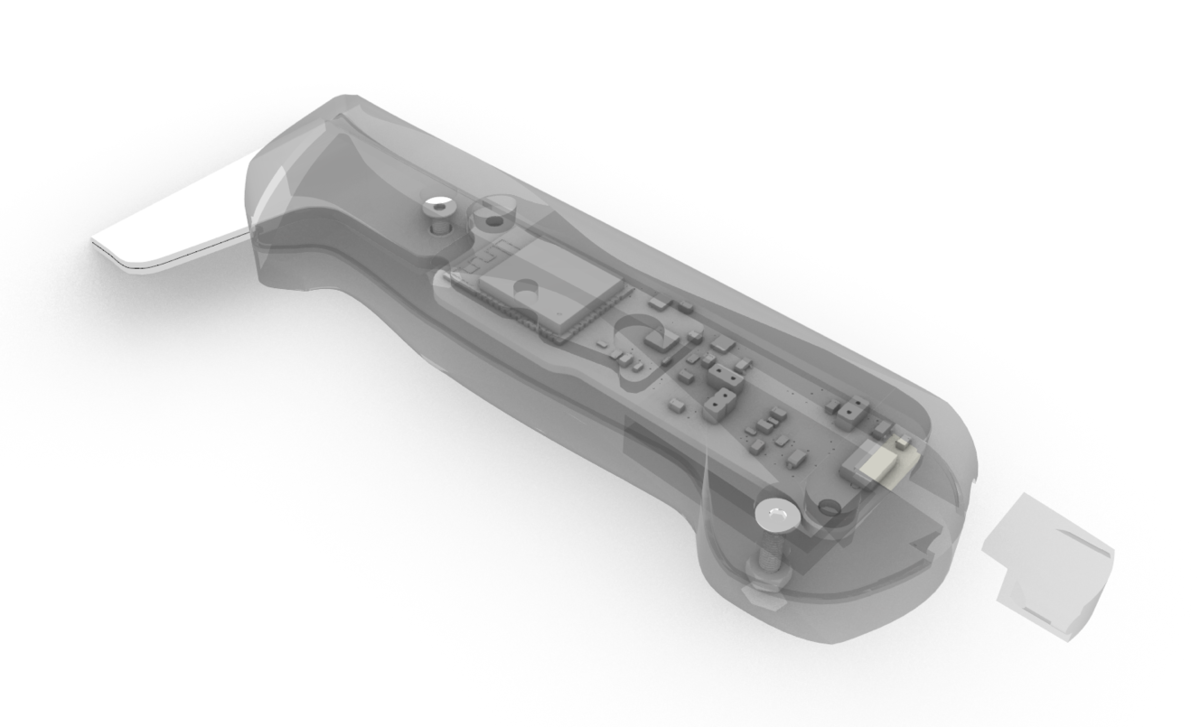
Next I needed to design a handle around the tang of my particular knife that could also accommodate my board, its battery (a small LiPo from AliExpress), and the small haptic feedback motor.
The first step was to gather measurements of the knife tang. I've found one of the best ways to digitize a roughly-planar object is to place it on a flatbed scanner. Scanners have a reasonably deep depth of field and high resolution.
Scanning the knife worked beautifully (this image is compressed; the actual one had much higher resolution):
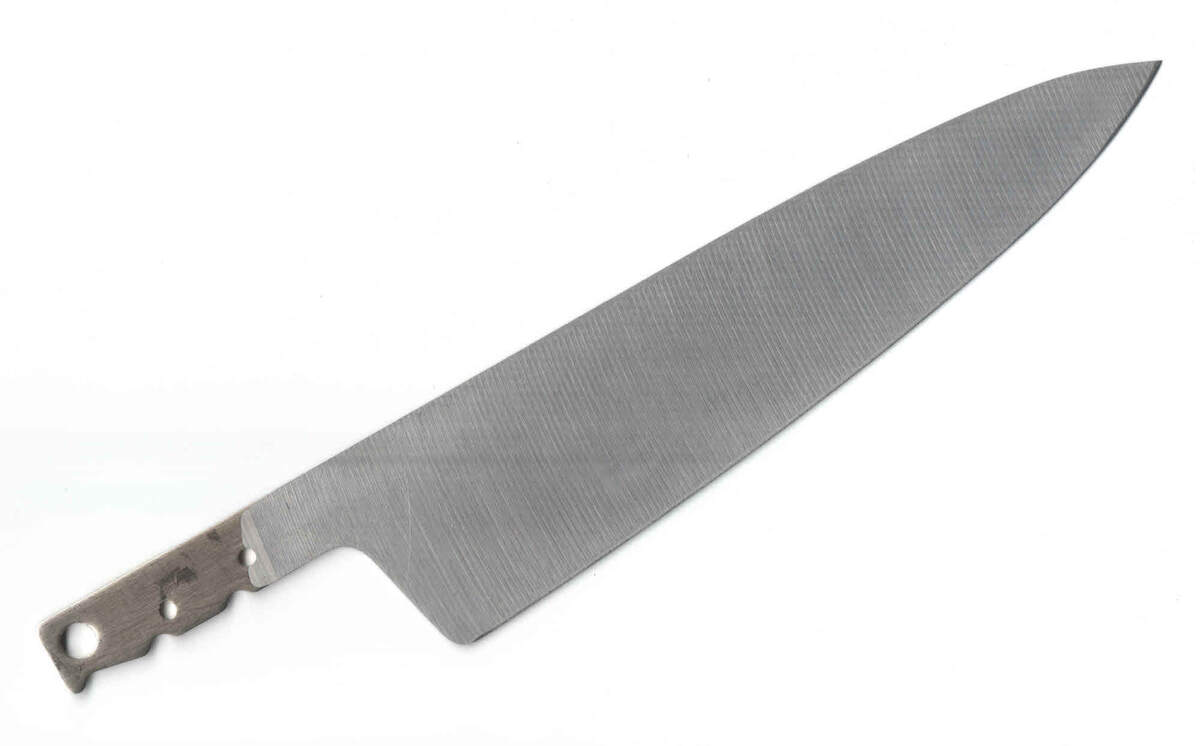
Once I had a digital copy of the knife to modify, I imported it into Rhino, rotated it to be horizontal, and scaled it so a single measurement I made in the real world (the height of the tang) matched the dimension of the same feature in its digital copy. This made sure the knife was dimensionally-accurate.
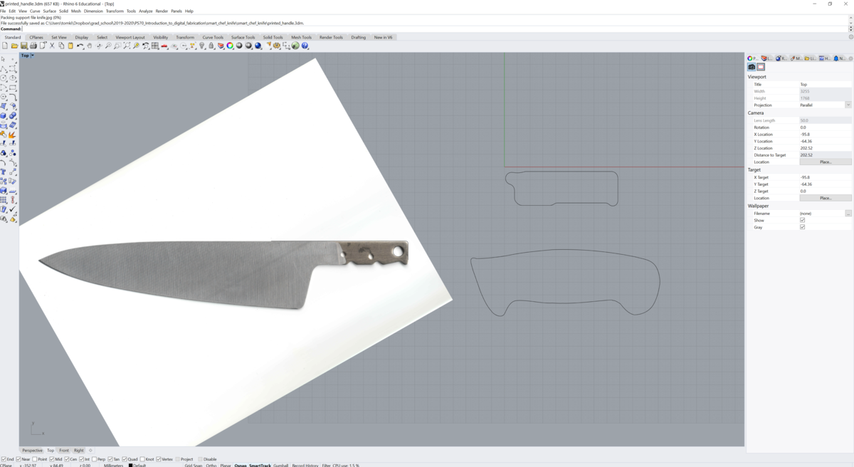
From there I imported my original hand-drawn handle outline, as well as the edge cut layer from KiCad for the version of the board I had fabricated. I played with the curves a bit and settled on a handle outline somewhere between the size of the board and the bulbous outline I first drew:
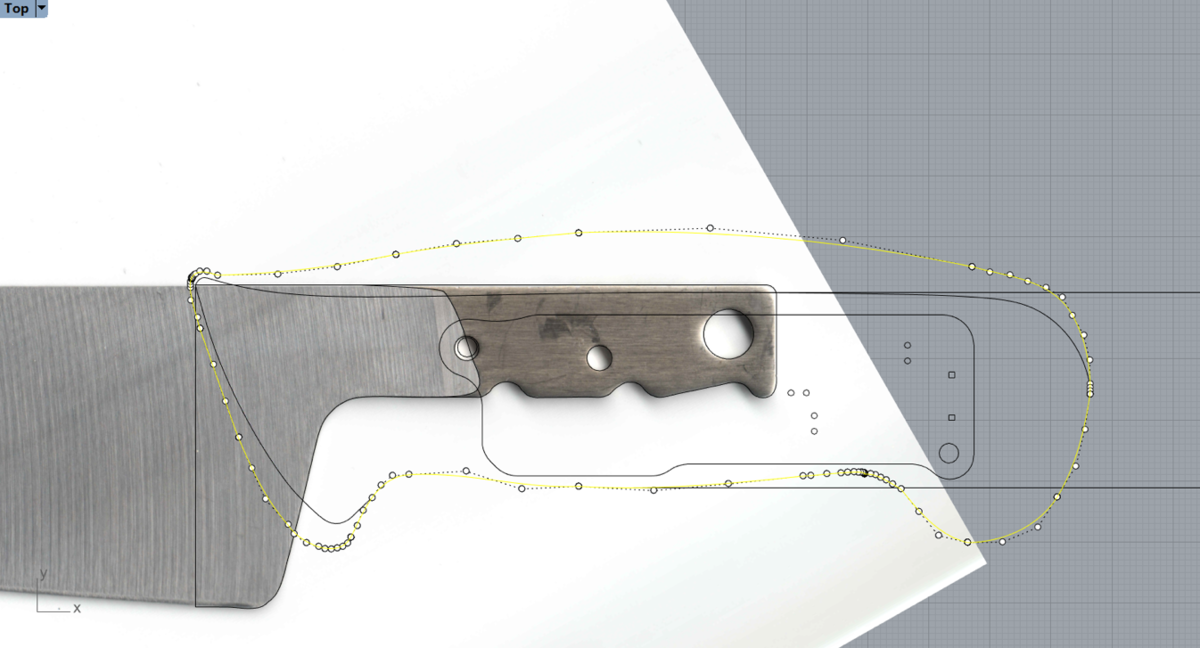
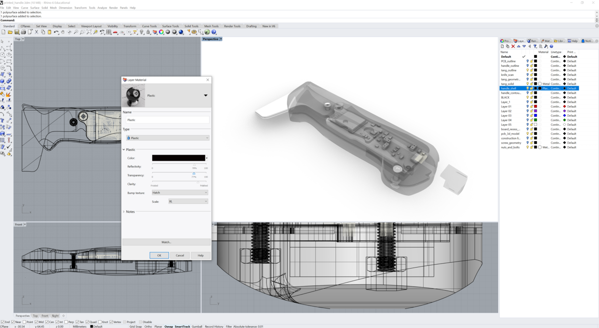
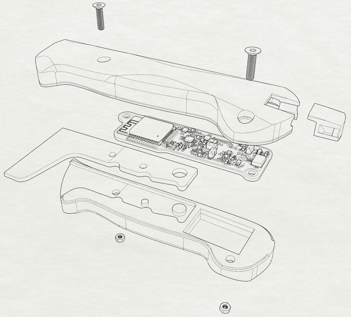
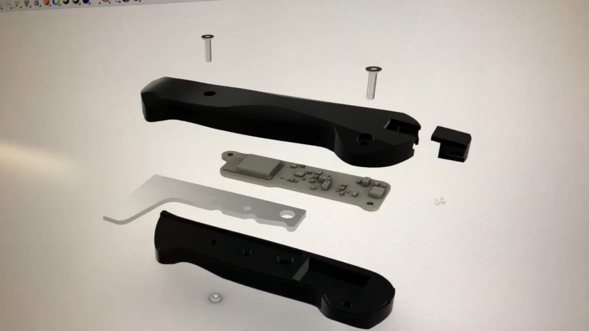
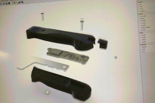
The outline was extruded to handle thickness, trimmed from all of the cardinal viewports to have the contour of a knife handle, split in half, and hollowed out to accommodate the board and battery.
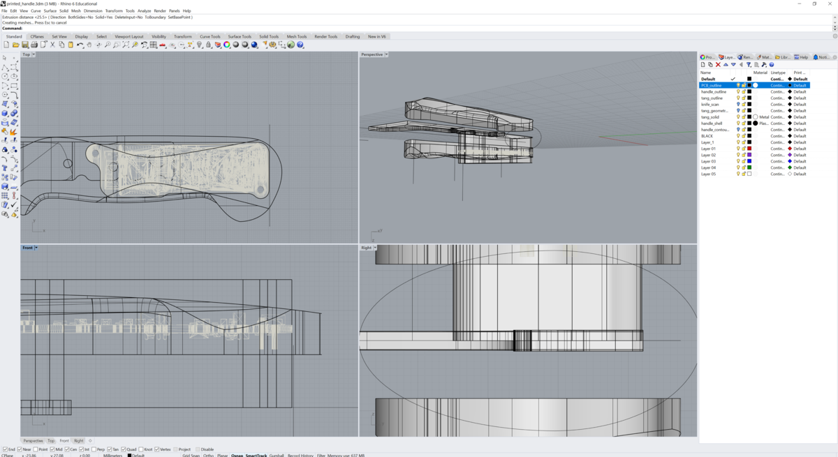
I added a removable door for the USB connector, and imported the 3D model from KiCad to get a sense of dimensions and clearances. Everything fit!
I added a few nuts and bolts to hold it all together: M3 M3x12 low-profile screws with 100º heads, McMaster part number 90729A169, with nut to match, part 94150A325.
Handle fabrication and assembly
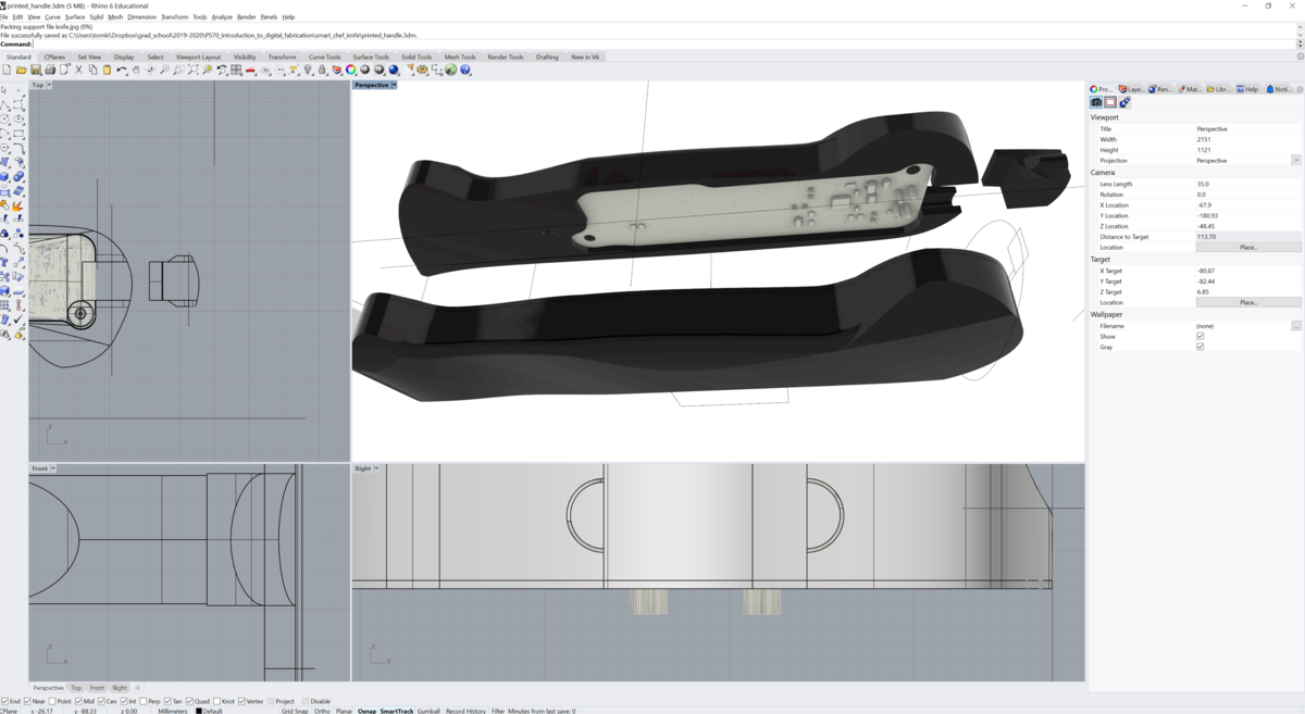
With the handle design at a reasonable point, I exported it as an *.stl file and sliced it for 3D-printing using PrusaSlicer:
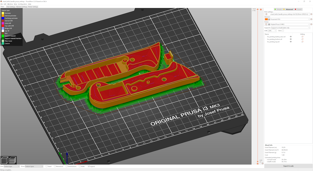
My wife's colleague generously printed the model using his Prusa i3 printer.
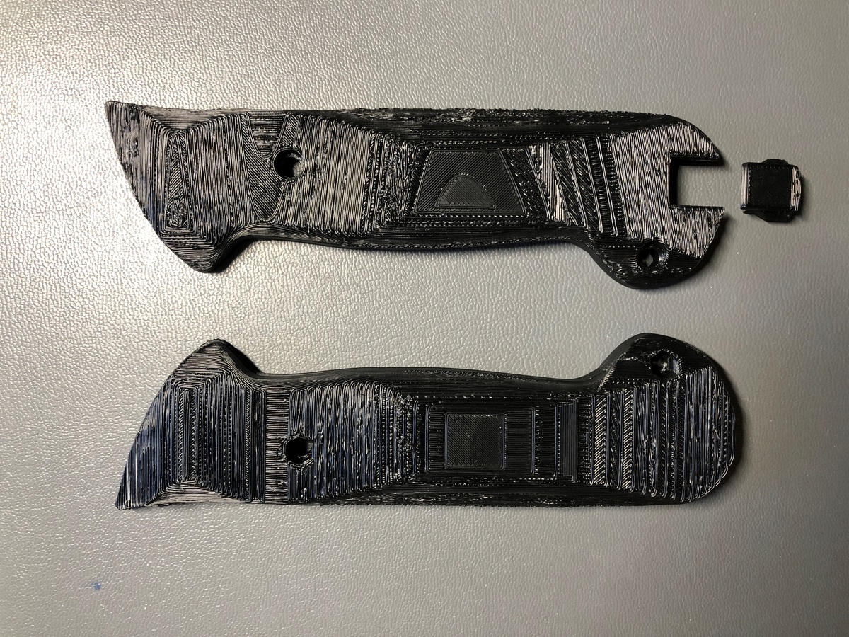
The PCB fits snugly, with 0.5mm of clearance planned around its perimeter.
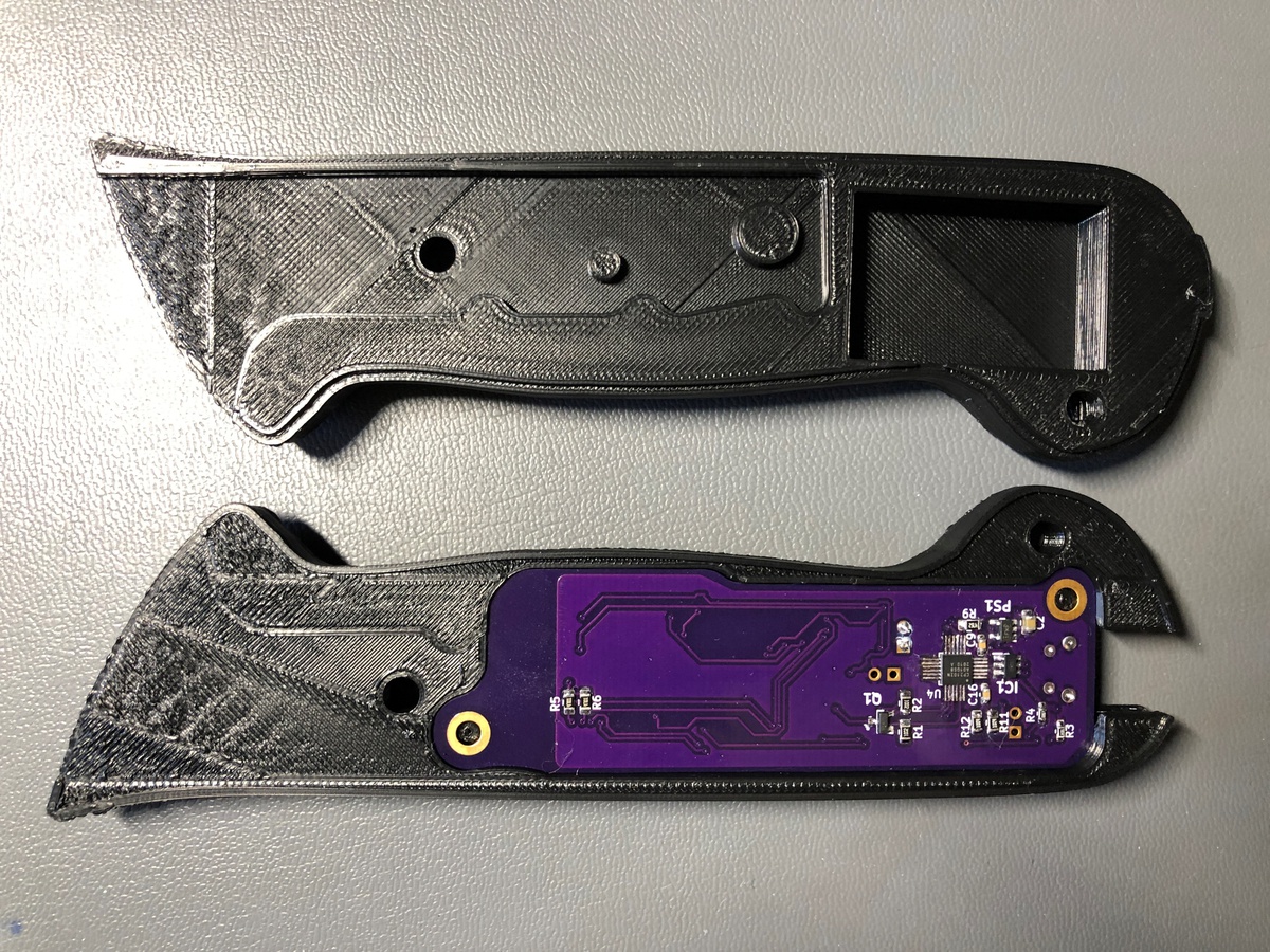
The knife tang fit as well, though very tightly (by design).
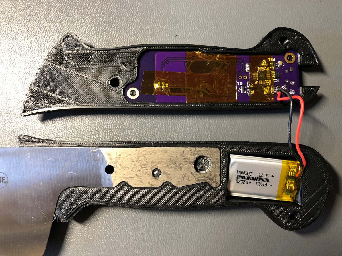
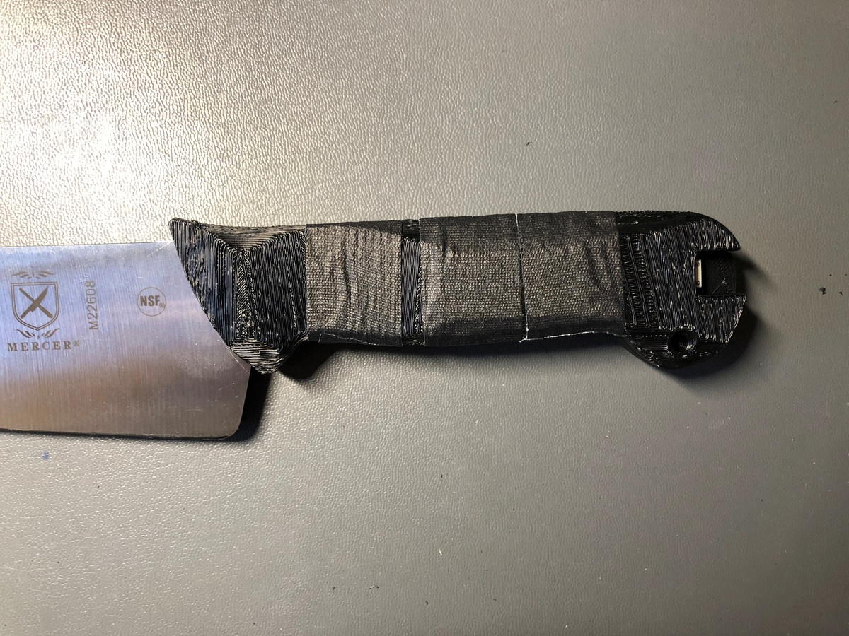
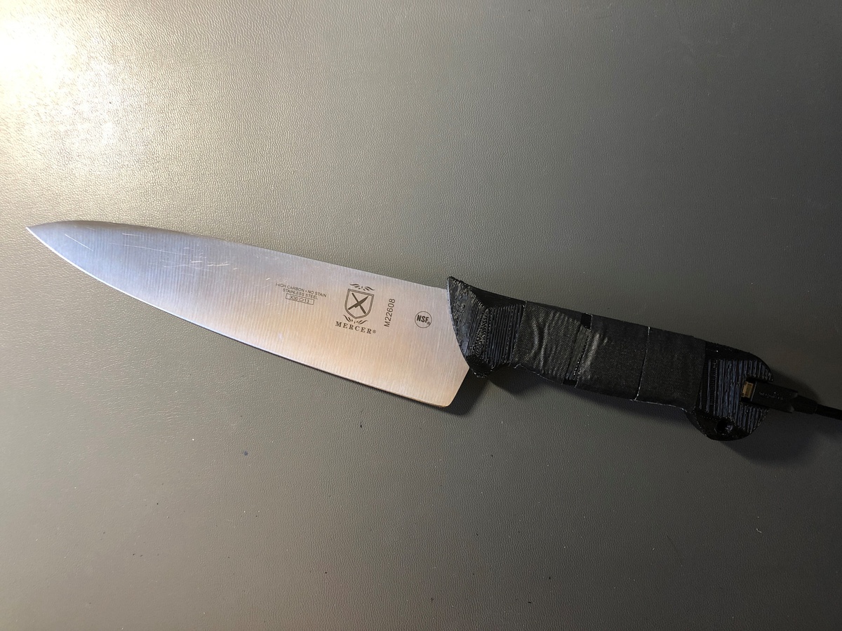
I did not have the planned screws from McMaster to attach the two halves, so black gaffer tape held them together temporarily.
Code for knife
Due to the late arrival of the PCBs from OSH Park, the software for this project was admittedly quite rushed and only demonstrates functionality of the hardware and basic use cases.
To interface with the MPU-6050 accelerometer/gyroscope, I used the https://github.com/rfetick/MPU6050_light library, which helpfully implements routines to obtain the current angle using the complementary filter.
The code for the knife is as follows:
Code for server
Code for the server can be found here.
The server side is implemented in Python with Flask. The conda environment for the flask dependencies are as follows:
name: flask-env
channels:
  - conda-forge
  - bioconda
  - defaults
dependencies:
  - _libgcc_mutex=0.1=main
  - ca-certificates=2020.1.1=0
  - certifi=2020.4.5.1=py37_0
  - click=7.1.2=py_0
  - flask=1.1.2=py_0
  - itsdangerous=1.1.0=py37_0
  - jinja2=2.11.2=py_0
  - ld_impl_linux-64=2.33.1=h53a641e_7
  - libedit=3.1.20181209=hc058e9b_0
  - libffi=3.3=he6710b0_1
  - libgcc-ng=9.1.0=hdf63c60_0
  - libstdcxx-ng=9.1.0=hdf63c60_0
  - markupsafe=1.1.1=py37h7b6447c_0
  - ncurses=6.2=he6710b0_1
  - openssl=1.1.1g=h7b6447c_0
  - pip=20.0.2=py37_3
  - python=3.7.7=hcff3b4d_5
  - readline=8.0=h7b6447c_0
  - setuptools=46.2.0=py37_0
  - sqlite=3.31.1=h62c20be_1
  - tk=8.6.8=hbc83047_0
  - werkzeug=1.0.1=py_0
  - wheel=0.34.2=py37_0
  - xz=5.2.5=h7b6447c_0
  - zlib=1.2.11=h7b6447c_3
prefix: /home/$(whoami)/miniconda3/envs/flask-env
The server can be dynamically started via:
FLASK_ENV=development FLASK_APP=app.py flask run --host=0.0.0.0
Design files for knife handle
The Rhino file for the knife handle design can be found here.
The STL files for the file can be found here: top, bottom, battery door.
KiCad design files
The KiCad design files can be found here.
Future work
- Pull as well as push for information from the knife to the server
- Sending of data vector/buffer rather than single accelerometer+gyro readings
- Gesture detection
- Instructional coaching, with step-by-step guidance on orientation changes
- Putting the ESP32 and haptic motor driver ICs to sleep to conserve energy, with interrupt-based wakeup initiated by the MPU-6050 accelerometer when motion is detected
- Recesses at the case seams to accomodate a rubber O-ring or other weather seal
- Conformal coating of the PCB to improve water resistance
- Experimenting with capacitive coupling of an ESP32 GPIO pin to the blade to detect food contact
- haptic feedback to detect unsafe practices
- when the knife notices it is slicing toward the user (requires awareness of left or right-hand use), when slips are detected, or when impacts are detected that may damage the knife edge
- pairing via bluetooth with a device that can configure Wi-Fi settings and preferences, send motion data via bluetooth